
EMF Protection: Does Copper Block EMF? Discover How Molded Copper Solutions Offer Shielding Advantages
In my years of working with electrical components, especially those used in the aerospace and telecom sectors, I’ve learned a thing or two about materials science and electromagnetic field (EMF) shielding. The question “does copper block EMF?" is not only frequently searched, it’s critical to understanding how to effectively manage electromagnetic interference.
Copper is an age-old material—trusted and relied on in various industrial applications for generations. In more recent years, mould base systems have emerged, especially when designing custom shielding solutions where performance and form-factor meet. In fact, base molding technologies paired with molded copper can enhance product durability and functionality in complex applications like IoT hubs, radar units, and even EV charging modules.
This article explores in depth why copper continues to be a popular shield, but also delves into what I discovered through trial runs—specifically regarding its copper block oxidation risks. Spoiler alert: even the best conductive metals need careful handling. Read along to understand why moldable copper forms offer new value—and whether that fits what you’re trying to solve.
---Why Does Copper Have Value in EMF Shielding?
Before jumping straight into does copper block emf, I think understanding **how EMF protection works in general** helps. Most EMF shielding methods operate on either reflectance or absorbance—copper tends to dominate via its **reflection property**.
- High Electrical Conductivity: Copper’s conductance rating (59.6 MS/m at room temp) places it right behind silver but above other cheaper conductors like aluminium
- Limited Signal Penetration: When designed correctly using the skin depth concept, high freq signals get reflected off without passing deeply inside the barrier
- Versatility in Molding: From standard plates to highly customized shields via plastic-injection backed copper layers (read: mould base) configurations are possible.
But as much as copper’s great conductivity helps with signal redirection, there are real-world considerations such as geometry limits (curvilinear parts might still require alternative metals). More on shapes later!
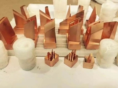
---Molded Copper Shields and Their Growing Role in Electronics Manufacturing
During testing with prototype enclosures for next-gen servers, I found that standard flat stamped sheet designs simply didn’t fit the contours of modern PCB layouts packed into slim housings anymore.
Using **Base Molding technology**, we created hybrid shields combining copper alloy shells bonded over flexible thermoplastics. It made the whole structure conformal yet strong enough for vibration-heavy applications.
Bonus advantage: thermal distribution. Since copper conducts heat well, these shields often doubled as part of the unit’s cooling mechanism—a win-win in compact device design.
 ---
---
Critical Performance Comparison Chart of Common Shield Metals
| Metal | EMF Reflectiveness @ 3GHz | Oxidation Susceptibility | Moldability Rating* |
|---|---|---|---|
| Copper | 95%+ | Medium–High (especially moist conditions) | Moderate** (with backing layer) |
| Aluminum | 82%–90% | Low | Excellent |
| Steel | <75% | High (without coating) | Okay (limited flex) |
*Moldability here refers to feasibility for integration within molded bases like ABS, PBT compounds.**Requires internal plating/overmold support.
---Oxidation Woes: What Happens With Exposed Surfaces in Humid Environments
If you leave your copper piece in a bathroom with poor ventilation, guess what—you’re going to deal with surface oxidants forming greenish deposits commonly referred to as tarnishing.
A case happened while designing protective casings for a water-cooled edge computing setup in Dallas (hot summers, plenty of condensation issues). Despite perfect solder contacts early during trials, weeks after exposure near HVACs the contact surfaces started corroding rapidly due to trapped moisture under casing seams.
- Rusting not common for copper per se—more accurately, copper block oxidation forms patinas instead
- Tin-based or epoxy coatings reduced this issue, though increased thickness
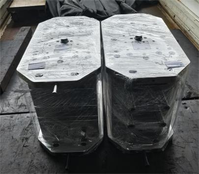
The Role of Mould Bases in Improving Long-Term Viability of Shielded Components
I’m biased towards mold-based construction because once you set up the molds and validate tool wear, repeatability hits near perfection, making production scalable. Even if minor tweaks are required for specific geometries.
Key benefits based on real prototyping feedback:
- Custom shape retention—even around irregular edges on modular PCBAs (printerd circuit assemblies)
- Reduces post-processing labor needed vs cutting/stamping approaches
- Easier to maintain consistency across large volume production runs—especially in base molding setups that use robotic arm dispensing for glue points
Common Applications and Use Cases Where Copper Still Dominates Over Alternatives
| Industry Segment | Purpose of Copper Use | Type Used |
| SATCOM Equipment Enclosires | Preventing external EM waves from distorting data links | 99.98% pure electroformed |
| MED Devices - ECG Monitors, PACS | Critital path shielding around sensors avoiding false alarms | Beryllium copper composites |
| Fiber Optic CPE Housings | Shield SFP ports / optics from EMI sources in urban centers | Thin-filament pressed strips |
Should You Invest Now in Custom-Mould Shield Options?
In summary: For complex designs, yes—it's hard beating mould based fabrication’s scalability once NRE (non-recurring engineering costs) break even by production batch #15 onwards. But if dealing solely with lab equipment needing rectangular boxes? Stamped copper may make better sense short term
I learned this firsthand through cost modeling: investing $22,450 in initial mold development got our team past phase 2 of regulatory trials faster than buying stock shielding cans every three months just for A/B test variations. That kind of efficiency saves time and nerves in fast-paced startup R&D spaces too.
- Check if the environmental factor will cause oxidation. Plan for protective treatments accordingly.
- Analyze component geometry—stepped transitions may need 3D print samples before tool investment lock-ins.
- Contact几家(Chinese transliteration for companies)manufacturers specialized in injection molded copper. Get their feedback before signing long-term POs.